As semiconductor manufacturing enters the nanometer era, wafers, as the core carriers of chips, directly determine yield and cost through their positional accuracy and angular consistency during processing and transportation.
Throughout slicing, grining, coating, dicing, pre‑packaging alignment and other processes, wafers are prone to tiny offsets, angular tilts and trajectory deviations due to mechanical vibration, transmission errors and tooling deviations. Even micron‑level deviations can lead to mass issues such as cutting chipping, overlay offset and bonding failure, severely restricting production capacity and yield improvement. Traditional mechanical positioning and manual alignment methods feature low accuracy and slow response, failing to adapt to high‑speed mass production and meet the requirements of advanced processes.
Against this backdrop, Lanbao CCD wire diameter correction sensor has become a core supporting device for precise alignment and deviation correction in semiconductor wafer manufacturing processes, with its core capabilities of non-contact, high precision and dynamic real-time correction. It provides reliable guarantees for automated precision production.

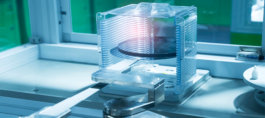
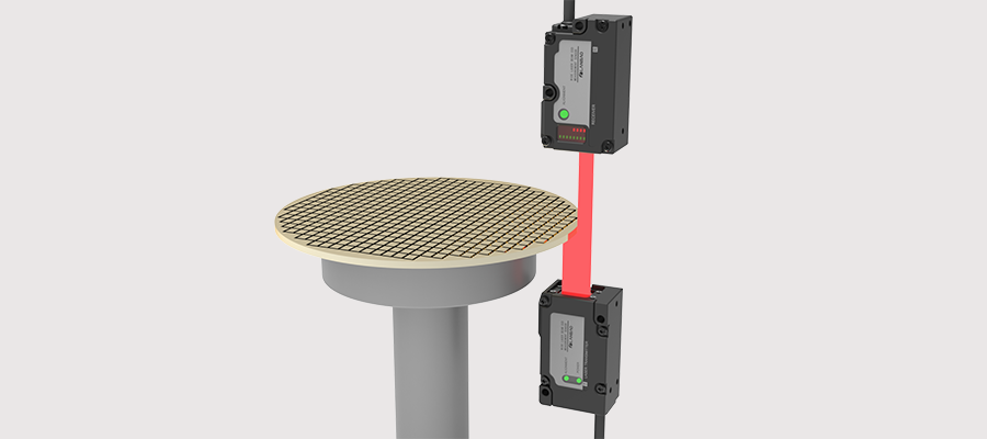
During operation, the transmitter generates a uniform parallel light curtain covering the wafer edge. The receiving-end CCD matrix captures the blocked light-dark boundary, outputs wafer offset values in real time, feeds them back to the production line control system, and drives the UVW platform to complete millisecond-level dynamic correction, forming a closed-loop control of measurement – calculation – correction. The entire process only performs data-based position sensing, with no photography, imaging or defect detection. It delivers faster response, stronger stability and lower cost, perfectly matching semiconductor mass production scenarios.
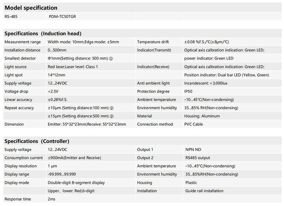
Lanbao CCD wire diameter correction sensor has undergone targeted optimization, achieving an ultra-high collection accuracy of ±1 μm, which can precisely capture tiny displacements and angular deviations of 8/12-inch wafer edges. Equipped with a dynamic temperature drift compensation algorithm, it boasts a temperature coefficient as low as ±8 μm/℃, effectively resisting workshop temperature fluctuations, minor vibrations and dust interference. It maintains stable data without drift or calibration errors during long-term continuous operation. Supporting 24/7 uninterrupted high-speed dynamic correction, it ensures nanometer-level alignment accuracy while significantly improving production line flow efficiency, balancing precision and efficiency.
With years of accumulated industrial sensing technology, Lanbao CCD wire diameter correction sensor offers three core advantages in wafer correction, precisely meeting the rigid demands of semiconductor mass production:
• High‑precision dynamic correction: Collects edge wire diameter and position data in real time, with millisecond‑level response for deviation correction. It eliminates the lag of static alignment and adapts to high‑speed automated production lines.
• High stability and anti‑interference operation: Equipped with an anti‑glare filter module, it operates stably under 3000 lux illumination, adapting to the high‑cleanliness and highly interferential working conditions of semiconductor workshops.
• Non‑contact and damage‑free adaptation: Adopts optical light curtain non‑contact measurement, avoiding contact with the wafer surface and edge. It completely prevents scratches and extrusion damage to ultra‑thin wafers (≤200 μm), ensuring wafer integrity.
Currently, Lanbao CCD wire diameter correction sensor is widely used in key processes such as wafer pre‑alignment, assembly line transmission correction, pre‑dicing alignment and pre‑packaging positioning. It can perform real‑time position deviation monitoring, data feedback and dynamic correction closed‑loop control, ensuring wafers maintain standard processing positions and transmission trajectories throughout the process. It fundamentally resolves mass production issues like defective products, material losses and process rework caused by alignment offsets. Measured data shows that with the Lanbao CCD correction solution, manual calibration costs are reduced by 80%, and equipment downtime is significantly cut, helping enterprises achieve dual goals of cost reduction, efficiency improvement and quality upgrading.
PDM Laser CCD Wire Diameter Measurement Sensor
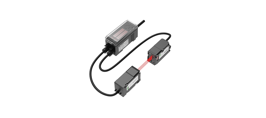
• Exquisite design, lightweight aluminum housing, easy for installation and removal
• Convenient operation panel with intuitive digital display
• Compact sensor and controller, saving installation space
• Wide measurement range with high precision, multiple measurement modes available
• Rich functions, easy configuration, wide range of applications
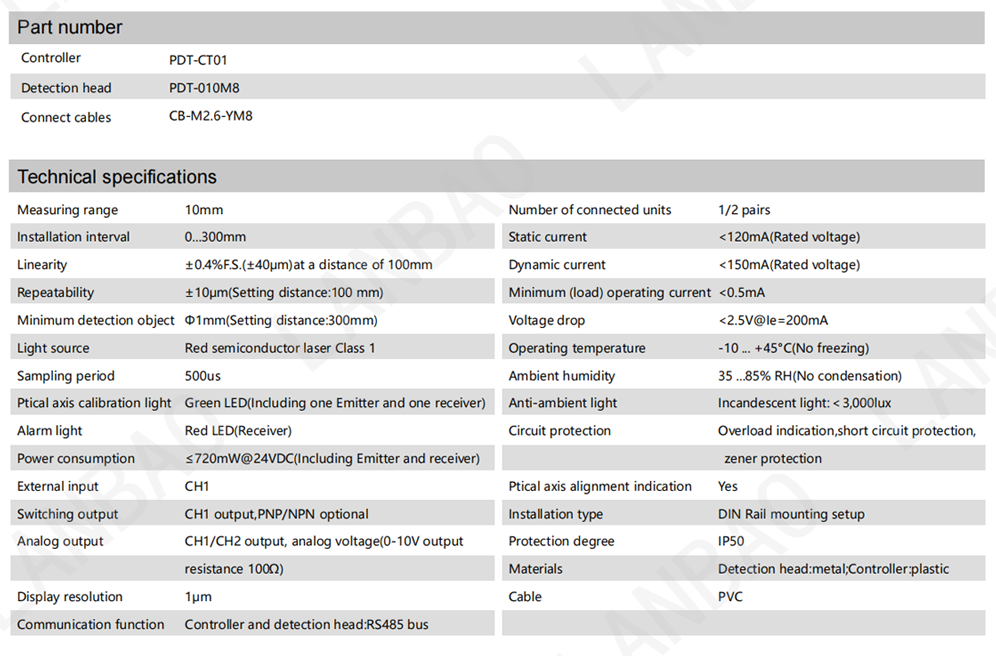
PDT Photoelectric Ranging Sensor
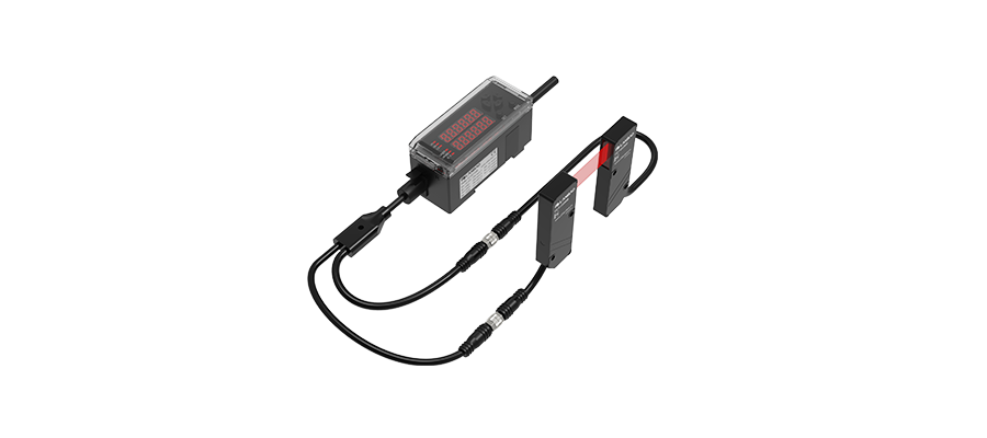
• Compatible with one‑to‑two connection, multi‑controller cascading and EtherCAT networking
• Wide range, high‑precision measurement with multiple modes available
• Exquisite design, sturdy and lightweight aluminum housing
• Convenient operation panel with dual digital display
• Optical axis alignment indicator for easy installation and alignment
As a high‑tech enterprise deeply engaged in industrial sensing, Lanbao Sensing focuses on addressing pain points in semiconductor intelligent manufacturing and developing correction and ranging sensing devices tailored for high‑end manufacturing. Its CCD wire diameter correction sensor is customized exclusively for wafer precision processing scenarios, precisely meeting the high‑precision, high‑stability and high‑reliability mass production standards of the semiconductor industry. Supporting the EtherCAT industrial bus, it can seamlessly connect to various automated wafer production lines. In the future, Lanbao Sensing will continue to deepen its presence in the semiconductor sector, iteratively optimize sensing correction technology and product performance, and empower the large‑scale, precise and efficient upgrading of China’s semiconductor industry with robust industrial sensing capabilities.
Post time: Jun-10-2026