Semiconductor manufacturing stands as one of the most precision-demanding and technologically complex fields in today's high-tech industry. As chip processes advance toward 3nm and even smaller nodes, the accuracy of measurements for wafer thickness, surface flatness, and microstructure dimensions directly determines chip yield and performance. In this context, laser displacement sensors, with their non-contact operation, superior precision, faster response times, and enhanced stability, have become indispensable "measurement eyes" throughout the semiconductor manufacturing process.
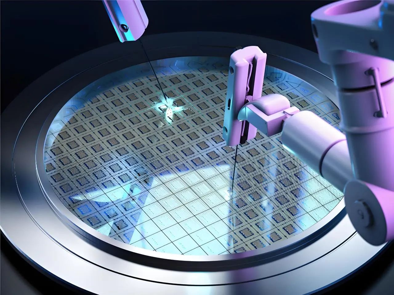
As the core substrate of semiconductor device fabrication, wafers require extreme precision and reliability during production. Among the many critical stages of wafer manufacturing, accurate displacement measurement is paramount—it directly impacts the final chip's performance and yield. As an innovation leader in China's industrial sensing sector, Lansensor's PDE series laser displacement sensors, featuring micron-level resolution, intelligent algorithms, and industrial-grade reliability, have emerged as the preferred solution for wafer manufacturing processes.
Precision Challenges in Wafer Manufacturing and the Advantages of Laser Displacement Sensors
Wafer manufacturing involves a series of complex processes such as photolithography, etching, thin-film deposition, and bonding—each requiring stringent precision at the micrometer or even nanometer level. For example:
-
In photolithography, precise alignment between the photomask and wafer is critical to ensure accurate pattern transfer onto the wafer surface.
-
During thin-film deposition, exact control of film thickness is essential to guarantee the electrical performance of devices.
Even the slightest deviation can lead to product defects or even render an entire batch of wafers unusable.
Traditional mechanical measurement methods often fall short in meeting such high-precision demands. Moreover, they risk damaging or contaminating the fragile wafer surface, while their slow response speeds make them inadequate for cutting-edge metrology requirements.
Lanbao sensor PDE Series Laser Displacement Sensors: The Optimal Solution for Wafer Applications
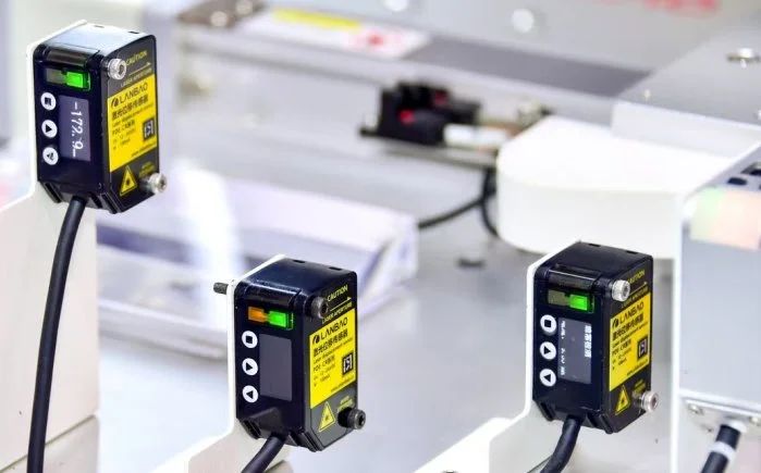
◆ Non-contact Laser Measurement
Utilizes laser beam projection onto target surfaces, analyzing reflected/scattered signals to obtain displacement data - eliminating physical contact with wafers to prevent mechanical damage and contamination risks.
◆ Micron-level Precision
Advanced laser technology and signal processing algorithms deliver micrometer-scale measurement accuracy and resolution, meeting the extreme precision demands of wafer fabrication processes.
◆ Ultra-fast Response (<10ms)
Enables real-time monitoring of dynamic production variations, allowing immediate deviation detection and correction to enhance manufacturing efficiency.
◆ Exceptional Material Compatibility
Capable of measuring diverse materials and surface types with strong environmental adaptability, suitable for multiple semiconductor process stages.
◆ Compact Industrial Design
The compact form factor facilitates seamless integration into automated equipment and control systems, enabling intelligent process monitoring and closed-loop adjustment.
Application Scenarios of PDE Series Laser Displacement Sensors in Wafer Processing
Lanbao sensor PDE Series Laser Displacement Sensors: Critical Applications in Wafer Manufacturing
With exceptional performance, Lansensor PDE laser displacement sensors play vital roles across multiple wafer fabrication processes:
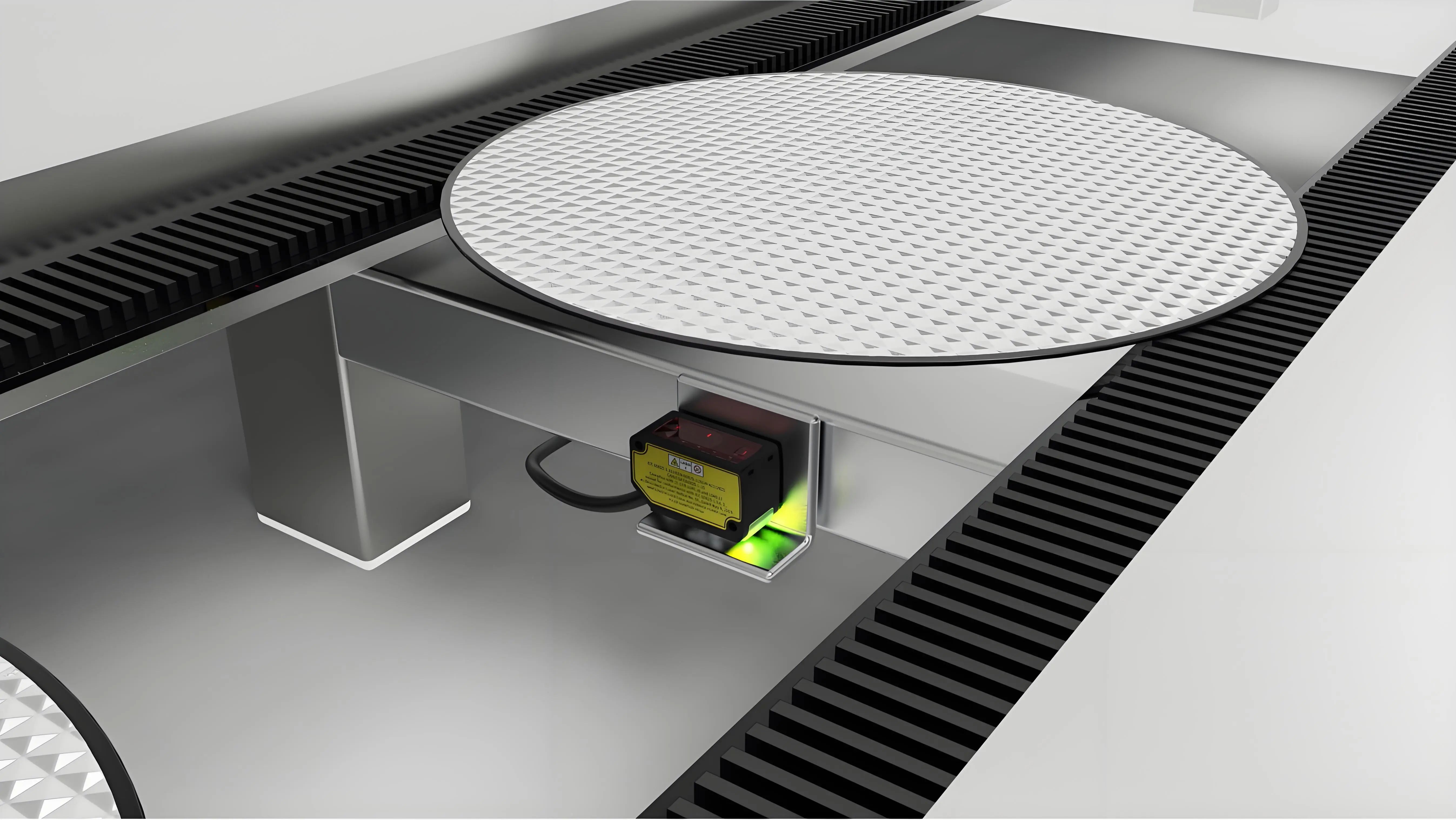
◆ Wafer Alignment & Positioning
For photolithography and bonding processes requiring micron-level accuracy, our sensors precisely measure wafer position and tilt angles to ensure perfect mask-to-wafer alignment and bonding arm positioning - enhancing pattern transfer precision.
◆ Wafer Thickness Metrology
Enabling non-contact thickness measurement with real-time monitoring during deposition processes, ensuring optimal thin-film quality control.
◆ Wafer Flatness Inspection
Detecting wafer warpage and surface deformation with sub-micron resolution to prevent defective wafers from progressing downstream.
◆ Thin-Film Thickness Monitoring
Providing real-time deposition thickness tracking during CVD/PVD processes to maintain strict electrical performance specifications.
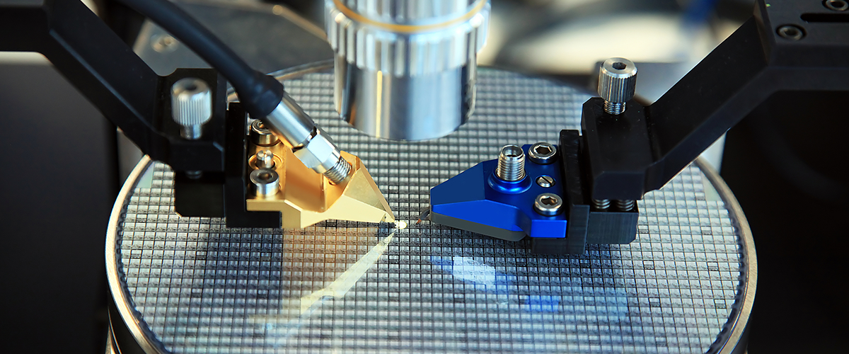
◆ Surface Defect Detection
Identifying micron-scale surface anomalies (scratches, particles) through high-resolution displacement mapping, significantly improving defect detection rates.
◆ Equipment Condition Monitoring
Tracking critical component displacements (robot arms, stage movements) and machine vibrations for predictive maintenance and stability optimization.
Lanbao sensor's PDE series not only bridges critical technology gaps in China's high-end industrial sensor market but establishes new global benchmarks with its exceptional performance. Whether boosting yield rates, reducing production costs, or accelerating next-gen process development, the PDE series stands as your ultimate weapon for conquering precision semiconductor manufacturing challenges!
Post time: May-08-2025