Kev tsim khoom siv semiconductor yog ib qho ntawm cov teb uas xav tau qhov tseeb tshaj plaws thiab nyuaj tshaj plaws hauv kev lag luam high-tech niaj hnub no. Thaum cov txheej txheem chip nce mus rau 3nm thiab txawm tias cov nodes me dua, qhov tseeb ntawm kev ntsuas rau wafer thickness, qhov chaw tiaj tus, thiab qhov loj me ntawm microstructure ncaj qha txiav txim siab qhov ntau thiab tsawg ntawm chip. Hauv cov ntsiab lus no, laser displacement sensors, nrog lawv txoj haujlwm tsis sib cuag, qhov tseeb zoo dua, lub sijhawm teb sai dua, thiab kev ruaj khov zoo dua, tau dhau los ua qhov tseem ceeb "qhov muag ntsuas" thoob plaws hauv cov txheej txheem tsim khoom siv semiconductor.
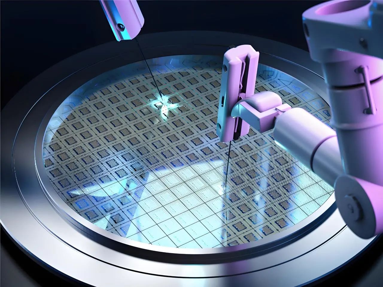
Raws li lub hauv paus tseem ceeb ntawm kev tsim cov khoom siv semiconductor, wafers xav tau qhov tseeb thiab kev ntseeg siab thaum lub sijhawm tsim khoom. Ntawm ntau theem tseem ceeb ntawm kev tsim wafer, kev ntsuas qhov hloov pauv yog qhov tseem ceeb - nws cuam tshuam ncaj qha rau qhov ua tau zoo thiab cov txiaj ntsig ntawm cov chip kawg. Ua tus thawj coj tshiab hauv Suav teb kev lag luam sensing, Lansensor's PDE series laser displacement sensors, uas muaj kev daws teeb meem micron-level, cov algorithms ntse, thiab kev ntseeg siab rau qib kev lag luam, tau tshwm sim ua qhov kev daws teeb meem nyiam rau cov txheej txheem tsim wafer.
Cov Kev Sib Tw Ua Ntej Hauv Kev Tsim Khoom Wafer thiab Cov Txiaj Ntsig ntawm Laser Displacement Sensors
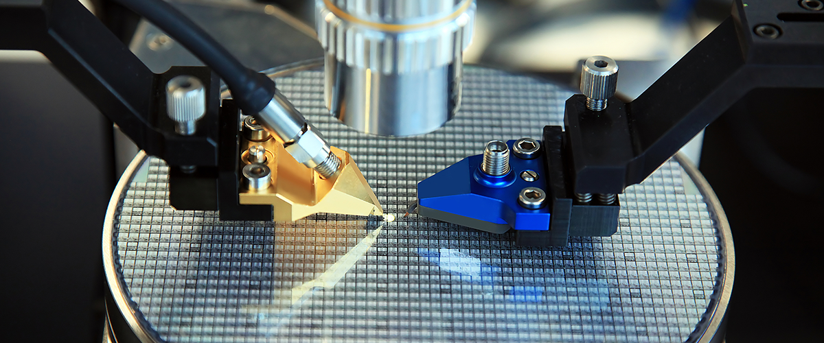
Kev tsim cov wafer muaj ntau yam txheej txheem nyuaj xws li photolithography, etching, thin-film deposition, thiab bonding—txhua yam xav tau kev ua kom raug ntawm micrometer lossis txawm tias nanometer. Piv txwv li:
-
Hauv photolithography, kev sib phim meej ntawm photomask thiab wafer yog qhov tseem ceeb heev kom ntseeg tau tias cov qauv hloov pauv raug rau ntawm qhov chaw wafer.
-
Thaum lub sijhawm tso cov zaj duab xis nyias, kev tswj kom meej ntawm cov zaj duab xis tuab yog qhov tseem ceeb kom lav qhov ua tau zoo ntawm hluav taws xob ntawm cov khoom siv.
Txawm tias qhov kev hloov pauv me me tuaj yeem ua rau cov khoom tsis zoo lossis ua rau tag nrho cov wafers tsis siv tau.
Cov txheej txheem ntsuas tshuab ib txwm muaj feem ntau tsis ua tau raws li qhov xav tau siab. Ntxiv mus, lawv muaj kev pheej hmoo ua rau puas tsuaj lossis ua rau lub wafer nto tsis ruaj khov, thaum lawv qhov kev teb qeeb ua rau lawv tsis txaus rau cov kev xav tau ntawm kev ntsuas niaj hnub.
Lanbaolub sensorPDE Series Laser Displacement SensorsKev daws teeb meem zoo tshaj plaws rau cov ntawv thov Wafer
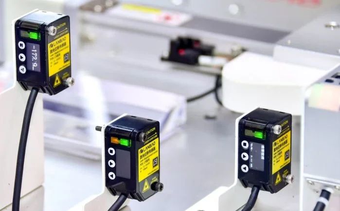
◆Kev Ntsuas Laser Tsis Sib Cuag
Siv cov teeb laser projection rau ntawm cov nto ntawm lub hom phiaj, tshuaj xyuas cov teeb liab uas tau cuam tshuam/cuam tshuam kom tau txais cov ntaub ntawv hloov chaw - tshem tawm kev sib cuag nrog cov wafers kom tiv thaiv kev puas tsuaj thiab kev pheej hmoo ntawm kev ua qias tuaj.
◆Kev Ntsuas Qib Micron
Cov thev naus laus zis laser siab heev thiab cov txheej txheem ua cov teeb liab xa cov kev ntsuas qhov tseeb thiab kev daws teeb meem ntawm micrometer, ua tau raws li qhov xav tau ntawm cov txheej txheem tsim wafer.
◆Cov Lus Teb Sai Sai (<10ms)
Ua rau muaj kev soj ntsuam tiag tiag ntawm cov kev hloov pauv ntawm cov khoom tsim tawm, ua rau pom thiab kho qhov sib txawv tam sim ntawd los txhim kho kev ua haujlwm ntawm kev tsim khoom.
◆Kev Sib Txuas Lus Zoo Tshaj Plaws ntawm Cov Khoom Siv
Muaj peev xwm ntsuas ntau yam khoom siv thiab hom nto nrog kev hloov pauv ib puag ncig zoo, tsim nyog rau ntau theem txheej txheem semiconductor.
◆Kev Tsim Kho Kev Lag Luam Me Me
Lub cev me me ua rau kev sib koom ua ke zoo rau hauv cov khoom siv tsis siv neeg thiab cov tshuab tswj hwm, ua rau muaj kev saib xyuas cov txheej txheem ntse thiab kev hloov kho lub voj voog kaw.
Cov xwm txheej ntawm daim ntawv thovPDE Series Laser Displacement Sensorshauv Wafer Ua
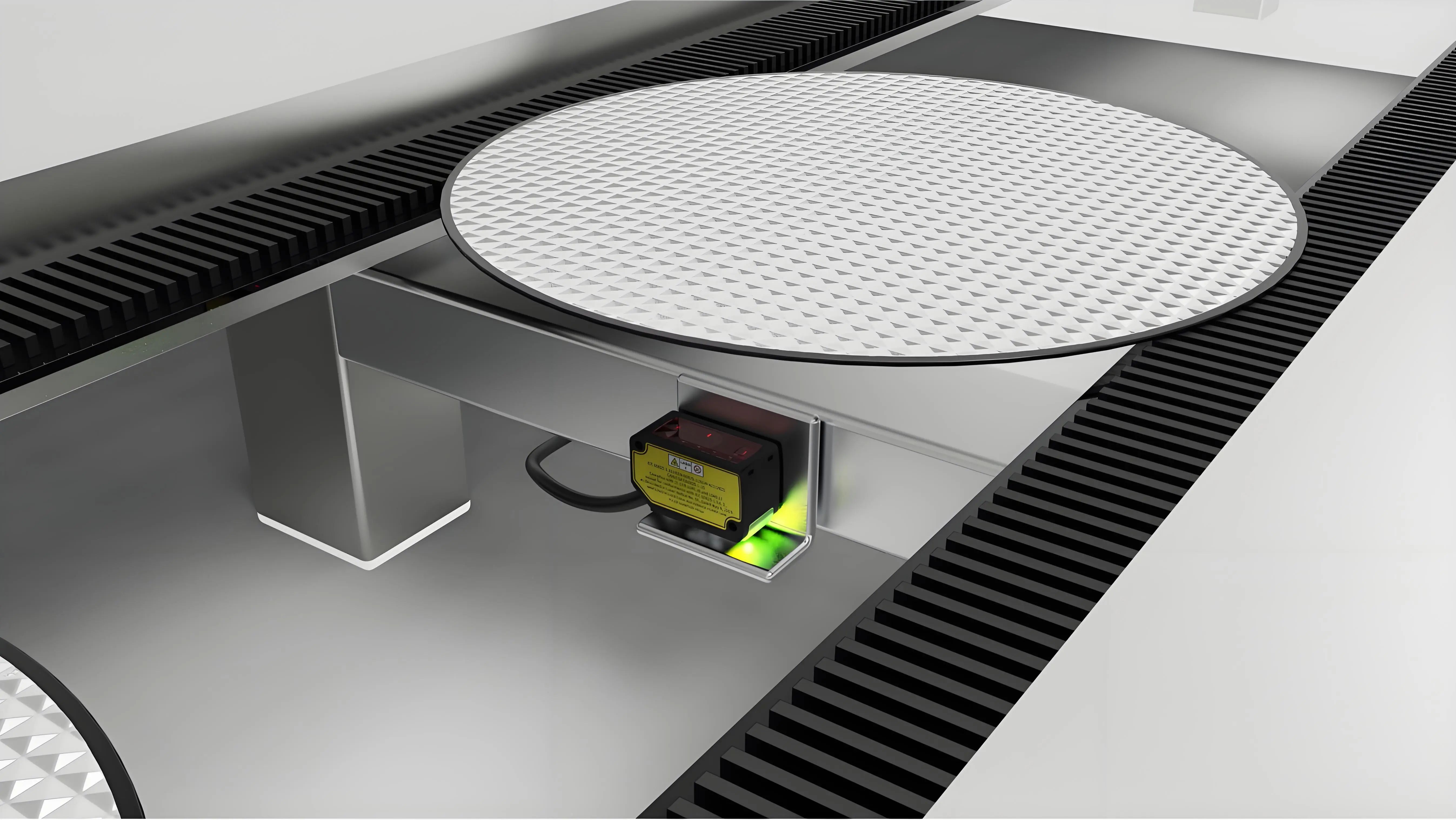
Lanbao sensorPDE Series Laser Displacement SensorsCov Ntawv Thov Tseem Ceeb hauv Kev Tsim Khoom Wafer
Nrog kev ua tau zoo tshaj plaws, Lansensor PDE laser displacement sensors ua lub luag haujlwm tseem ceeb thoob plaws ntau yam txheej txheem tsim wafer:
◆Kev Sib Tov thiab Kev Tso Chaw ntawm Wafer
Rau cov txheej txheem photolithography thiab kev sib txuas uas xav tau qhov tseeb ntawm micron, peb cov sensors ntsuas qhov chaw ntawm wafer thiab lub kaum sab xis kom ntseeg tau tias qhov sib phim zoo meej ntawm lub ntsej muag-rau-wafer thiab qhov chaw ntawm caj npab sib txuas - txhim kho qhov tseeb ntawm kev hloov pauv qauv.
◆Kev Ntsuas Qhov Ntev ntawm Wafer
Ua kom ntsuas qhov tuab tsis sib chwv nrog kev saib xyuas tiag tiag thaum lub sijhawm tso cov txheej txheem, kom ntseeg tau tias kev tswj hwm zoo tshaj plaws ntawm cov zaj duab xis nyias.
◆Kev Tshuaj Xyuas Qhov Sib Npaug ntawm Wafer
Tshawb nrhiav wafer warpage thiab deformation ntawm qhov chaw nrog kev daws teeb meem sub-micron kom tiv thaiv cov wafers uas puas lawm kom tsis txhob mus rau sab qis.
◆Kev Soj Ntsuam Thickness ntawm Zaj Duab Xis
Muab kev taug qab cov tuab ntawm cov khoom siv thaum lub sijhawm tiag tiag thaum lub sijhawm CVD/PVD kom tswj tau cov kev ua haujlwm hluav taws xob nruj.
◆Kev Tshawb Pom Qhov Tsis Zoo Ntawm Qhov Chaw
Txheeb xyuas qhov tsis zoo ntawm qhov chaw me me (cov khawb, cov khoom me me) los ntawm kev kos duab qhia chaw siab, txhim kho qhov nrawm ntawm kev kuaj pom qhov tsis zoo.
◆Kev Saib Xyuas Cov Khoom Siv
Taug qab qhov kev hloov pauv tseem ceeb ntawm cov khoom siv (caj npab neeg hlau, kev txav ntawm theem) thiab kev co ntawm lub tshuab rau kev kwv yees kev saib xyuas thiab kev ua kom ruaj khov zoo dua.
Lanbao sensor's PDE series tsis yog tsuas yog txuas cov qhov sib txawv tseem ceeb hauv kev lag luam sensor kev lag luam siab hauv Suav teb xwb tab sis tsim cov qauv tshiab thoob ntiaj teb nrog nws cov kev ua tau zoo tshwj xeeb. Txawm hais tias txhawb cov nqi tsim khoom, txo cov nqi tsim khoom, lossis ua kom nrawm dua cov txheej txheem tom ntej, PDE series sawv cev rau koj cov riam phom kawg rau kev kov yeej cov teeb meem kev tsim khoom semiconductor precision!
Lub sijhawm tshaj tawm: Tsib Hlis-08-2025